Current Work
Algorithmic Optimization of Nanophotonic Structures
I am currently working on techniques of utilizing algorithmic optimization (e.g. evolutionary optimization, inverse design, machine learning) to create nanophotonic devices with new or enhanced functionality. Due to the wave-nature of light at the nanoscale, optimal structures are often highly unintuitive, and thus traditional design techniques are limited in the performance they can achieve. Allowing algorithms to fully design nanophotonic structures allows effects like interference, and modification of the local density of optical states to be leveraged.
Previous Work
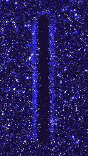
Super-resolution image of nanowire coupling to single-molecule emitters
Imaging Optical Interactions with Nanowires
While interactions between quantum emitters and nanostructures are increasingly well understood theoretically, experimental imaging of such interactions has proven quite challenging.
In this work we demonstrate a novel super-resolution microscopy technique, based on photo-activated localization microscopy (PALM). In contrast to traditional PALM measurements, we measure both the location and intensity of fluorophores stochastically adsorbed on and surrounding a nanostructure. This allows for direct, spatially resolved mapping of the interaction between dipole-like emitters and nanophotonic structures. First, through experimental measurements of nanowire-fluorophore interactions, we provide direct imaging of the photonic antenna effect responsible for the large absorption cross-sections of nanowire devices, particularly of interest to the fields of nanostructured photodetectors and photovoltaics. Second, the theoretical deconvolution of the observed signal into emission enhancement, directivity modifications, and waveguide coupling provides new insight into quantum emitter/nanostructure interactions, and is additionally applicable to the fields of single photon emission and nanoscale lasers. Finally, the demonstration of this new technique, along with prospective improvements or cooperation with other measurements, could allow for direct determination of specific individual properties (e.g. coupling, absorption) in future studies, on arbitrary nanophotonic devices. The work is available here.
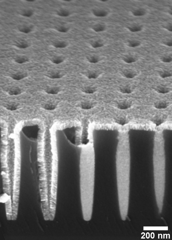
Nanohole Structured a-Si:H Solar Cell
Nanohole Structured a-Si:H Photovoltaics
In our previous studies, we found that the large number of fluctuating defects in a-Si:H seems to cause the hole mobility in such devices to be inherently limited.
In this work, we show that nanostructuring of devices can work around this limitation. Using the advantages of a-Si:H - its strong absorption and lack of detrimental surface states - we implement a nanohole structure filled with a transparent conducting AZO material. This allows the device to collect carriers through the nanohole surfaces, thereby improving the efficiency of the solar cell. In practice, we observe large improvements in performance, with the best devices going from 7.2 to 10.4%, close to the current record for single-junction a-Si:H materials (even without significant optimizations in layer thicknesses and composition), and confirm that this improvement is indeed occurring from enhancements in carrier collection. The work is available here.
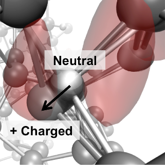
Hole wavefunction localization near a highly displacing silicon atom
Origins of Hole Trapping in Amorphous Silicon
While there exists an abundance of theories on the causes of structural hole traps in hydrogenated amorphous silicon (a-Si:H), there remains little consensus on their true origins. Through statistical analysis of an ensemble of 2700 virtual a-Si:H structures, I am able to probe the causal relationships between geometric phenomena and the presence of strong hole traps in the material. A variety of interesting correlations were determined, for example, the strongest observed causal link to hole trapping was the "ionization displacement," or amount of atomic movement present in a sample when positively charged. The work is available here.
From this point I am investigating methods of utilizing what we learned in the previous study to attempt to prevent the formation of the structural phenomena linked to strong hole trapping. One method I am are currently evaluating is the application of stress to the material, postulating that stress will change the relative benefits and penalties to ionization displacements, and thereby mitigating their formation.
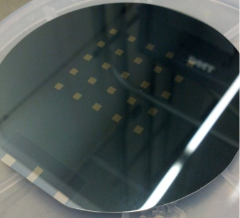
Amorphous silicon PIN-structure photvoltaic cells, used for measuring hole mobility in the material
Correlations between Deposition Parameters and Hole Mobility in a-Si:H
My first experimental project, determining the origins of stress in plasma enhanced chemical vapor deposited amorphous silicon, available here, in combination with the computational work mentioned above, led us to ask if the stress engineered in the films could be used to improve the hole transport.
To this end, I am investigating the influence of various structural properties (stress, density, hydrogen content and bonding configurations, for example), controllable via the deposition parameters, on the hole mobility of the sample. Through the use of a time-of-flight transient current measurement, we can determine the hole mobility directly in our samples.